

signal integrity in pcb production and assembly
Ensuring signal integrity is paramount in Printed Circuit Board (PCB) production and assembly to maintain the reliability and performance of electronic devices. Signal integrity refers to the ability of electrical signals to propagate through a PCB without distortion or degradation, ensuring accurate data transmission and proper functionality of the device. Achieving signal integrity requires careful consideration of various factors throughout the design, production, and assembly processes, as even minor deviations can lead to signal integrity issues such as signal loss, noise, and timing errors.
One crucial aspect of ensuring signal integrity in pcb production and assembly is adhering to proper design practices. Design considerations such as controlled impedance matching, signal routing topology, and signal integrity simulation play key roles in minimizing signal degradation and optimizing performance. Controlled impedance matching involves designing traces to maintain consistent impedance throughout the PCB, reducing reflections and signal distortions. Signal routing topology, including trace length matching, differential pair routing, and high-speed signal routing, helps minimize signal skew and ensure uniform signal propagation.
Moreover, signal integrity simulation tools, such as electromagnetic field solvers and signal integrity analysis software, enable designers to predict and analyze signal behavior before fabrication. By simulating signal propagation, crosstalk, and electromagnetic interference (EMI), designers can identify and address potential signal integrity issues early in the design process, optimizing layout and routing to ensure reliable performance.
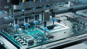
How do you ensure signal integrity in pcb production and assembly?
During PCB fabrication, maintaining signal integrity involves using high-quality materials and manufacturing processes. Selecting appropriate substrate materials with consistent dielectric properties and low loss tangents is essential for minimizing signal attenuation and distortion. Advanced fabrication techniques, such as controlled impedance manufacturing and fine-line lithography, ensure precise trace geometries and uniformity, contributing to optimal signal integrity.
In PCB assembly, proper component placement, soldering techniques, and thermal management are critical for preserving signal integrity. Careful component placement minimizes signal paths and reduces parasitic effects such as inductance and capacitance, which can degrade signal quality. Surface Mount Technology (SMT) assembly techniques, including reflow soldering and solder paste inspection, ensure reliable solder joints and minimize signal discontinuities. Additionally, thermal management measures such as heatsinking and thermal vias help dissipate heat generated by high-power components, preventing thermal-induced signal degradation.
Furthermore, rigorous testing and inspection are essential for verifying signal integrity throughout the production and assembly process. In-circuit testing (ICT), boundary scan testing, and high-frequency testing methods validate electrical connectivity, measure impedance, and verify signal quality. Automated Optical Inspection (AOI) and X-ray inspection systems identify defects such as solder bridges, opens, and misalignments that could compromise signal integrity. Functional testing and signal integrity validation under simulated operating conditions ensure that PCBs meet performance specifications and reliability requirements.
In conclusion, ensuring signal integrity in PCB production and assembly requires a holistic approach encompassing design, fabrication, assembly, and testing processes. By implementing proper design practices, using high-quality materials and manufacturing techniques, and conducting thorough testing and inspection, manufacturers and assemblers can minimize signal degradation and optimize performance. With signal integrity as a primary consideration, electronic devices can reliably transmit data and operate as intended, meeting the stringent demands of today’s high-speed and high-frequency applications.


