Pcb Assembly and Manufacturing Processes
PCB assembly is the process of mounting small components onto a circuit board in order to create an electronic device with a specific function. This is typically a manual process, though automated equipment is now used for many tasks. PCBs can be crafted in both rigid and flexible formats, depending on the specific requirements of the device. Rigid PCBs are common, and consist of a base material such as fiberglass or epoxies. Flex PCBs, on the other hand, are more flexible and may include materials such as Kapton plastic.
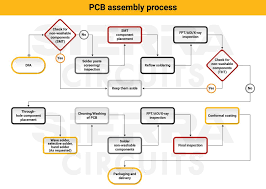
Regardless of the type of PCB being assembled, there are a few key steps involved. The first is preparing the substrate. This involves cleaning the surface of the substrate to ensure optimal adhesion, and then applying a copper layer through either a chemical or electroless deposition process. Next, a solder mask is applied to the substrate. This is a vital step, as it protects the substrate from heat and provides places for the addition of component leads. Finally, the circuit boards are sent to robotic pick and place machines, which add surface-mount components to the board.
Once the component placement has been completed, the PCB undergoes reflow soldering. This process uses high temperatures to melt the solder paste, forming reliable electrical connections between the components and the substrate. After reflow soldering, the circuit board is subjected to a visual inspection and functional testing, which ensures that all of the components are properly positioned and connected.
Types of Pcb Assembly and Manufacturing Processes
Another assembly method is through-hole (THT) technology, which involves insertion of components by way of holes in the circuit board. This method is ideal for devices that need to withstand significant mechanical stress, and can be done manually or with automated equipment. The through-hole assembly process is more complex than SMT, but it can offer a higher level of reliability and durability.
There are several different types of pcb assembly and manufacturing processes, but the most common is surface mount technology. This method utilizes automated equipment to place small, sensitive components onto the board. It can also be used to make changes to the design of the circuit board, such as adding more components or altering their positions.
Before the component placement process begins, the circuit board is etched with copper layers to create conductive pathways. Once this step is complete, a solder paste is applied to the surface of the substrate. A stencil is then used to apply the solder paste to the areas of the PCB where the components will be placed. The solder paste is a mixture of solder and flux, which helps to provide reliable electrical connections between the components and the substrate. The next step is the placement of the components, which can be accomplished with either manual or automated equipment. Finally, the board is reflow soldered and inspected before it is shipped to customers. This process can be time-consuming and expensive, but it is essential to the functionality of any electronic device.