EMI/RFI shielding incorporated into printed board assembly
Incorporating Electromagnetic Interference (EMI) and Radio Frequency Interference (RFI) shielding into printed board assembly (PBA) is essential for ensuring the performance and reliability of electronic devices. EMI/RFI shielding protects sensitive electronic components from external electromagnetic fields and prevents internal emissions from affecting nearby devices. This process involves several strategies, including careful design, material selection, and implementation of shielding techniques throughout the assembly process.
One fundamental approach to EMI/RFI shielding in printed board assembly is the use of ground planes. Ground planes are large areas of conductive material, typically copper, embedded within the PCB layers. These planes act as a reference point for all circuit grounds, reducing noise and providing a path for the return currents. By strategically placing ground planes adjacent to signal layers, designers can create a low-impedance path that helps minimize electromagnetic emissions and susceptibility.
Another critical aspect is the placement and routing of components and traces. High-frequency signals and noisy components, such as oscillators and switching power supplies, should be placed away from sensitive analog circuits. Proper trace routing ensures that high-speed signal paths are short and direct, minimizing the loop area and reducing the potential for radiated emissions. Additionally, using differential pairs for high-speed signals can help cancel out electromagnetic fields, further reducing EMI.
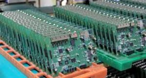
How is EMI/RFI shielding incorporated into printed board assembly?
Shielding can also be achieved through the use of metal enclosures or cans. These enclosures are typically made of conductive materials such as aluminum or copper and are placed over specific sections of the PCB to contain and block electromagnetic fields. Metal shields are particularly effective for high-frequency components and areas with dense circuitry. They can be soldered directly to the PCB, providing a robust and effective barrier against EMI/RFI.
In some designs, conductive coatings or paints are applied to the PCB surface or housing. These coatings contain metal particles that create a conductive layer, effectively shielding the board from electromagnetic interference. Conductive coatings are a flexible solution, as they can be applied to irregular surfaces and provide good coverage with minimal added weight or thickness. This method is especially useful for devices with complex shapes or limited space for traditional shielding methods.
The use of EMI/RFI gaskets and tapes is another effective technique. These materials are typically made from conductive elastomers or metal-filled fabrics and are used to seal gaps and seams in enclosures, ensuring continuous conductive paths. Gaskets and tapes can be applied to doors, covers, and other removable parts of the enclosure, maintaining the integrity of the shield while allowing for easy access to the PCB when needed.
PCB laminates with embedded shielding layers offer another advanced solution. These laminates incorporate layers of conductive material within the PCB stack-up, providing built-in EMI/RFI shielding without the need for additional external components. This approach is particularly beneficial for high-density and multilayer PCBs, where space is limited, and traditional shielding methods may be impractical.
Grounding and bonding practices are also crucial in effective EMI/RFI shielding. Ensuring that all parts of the PCB and the enclosure are properly grounded helps maintain a consistent potential and reduces the risk of electromagnetic interference. Using multiple ground vias and stitching them around the PCB perimeter enhances the effectiveness of the ground plane and minimizes ground loops, which can cause interference.
Testing and validation are essential to verify the effectiveness of EMI/RFI shielding. Techniques such as radiated emission testing, conducted emission testing, and susceptibility testing help identify potential issues and validate the shielding design. By performing these tests during the design and prototyping phases, engineers can make necessary adjustments to improve the shielding performance before moving to full-scale production.
In summary, incorporating EMI/RFI shielding into printed board assembly involves a combination of design strategies, material selection, and implementation of various shielding techniques. Ground planes, metal enclosures, conductive coatings, gaskets, tapes, embedded shielding layers, and proper grounding practices all play critical roles in minimizing electromagnetic interference. Thorough testing and validation ensure that the shielding measures are effective, resulting in reliable and high-performance electronic devices.