Soldering Utilized in Stacked Microvias
The PCB manufacturing process creates tiny holes, called vias, that connect different copper areas on the board. Vias are drilled and filled with solder or plated with copper to make the electrical connections between layers on your printed circuit board (PCB). Stacked microvias are a way to reduce the number of vias needed on your board, making it more compact and lowering material costs. Stacked microvias also provide less risk of crosstalk between traces, allowing you to design your board with more layers while maintaining high performance.
Stacked microvias are used when you have multiple layers in your board and need to reach a specific layer with the shortest path possible. In a standard PCB, a trace can pass between layers by running parallel to other traces in close proximity, but this increases the chance of crosstalk and reduces your circuit board’s efficiency. With stacked microvias, your traces are routed away from each other, reducing crosstalk between layers and minimizing the amount of EMI the traces generate.
To make a stacked microvia, a machine drills a series of small, circular, metallurgical via holes into the surface of the PCB. These are then stacked one on top of the other, with each hole having two narrow annular rings, one at the top and the other at the bottom. The top annular ring provides structured support for the via while the lower one makes the electrical connection.
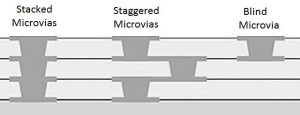
How is Soldering Utilized in Stacked Microvias?
After drilling, the machine fills each microvia with conductive paste and then plates them over with copper. The manufacturer uses a special type of copper plating to make strong, reliable connections at the via-to-pad interface. This process is known as copper wrap plating and is a critical part of the manufacturing process. However, over the past few years, there have been reports of failures that appear to be related to stacked microvias and copper wrap plating.
A key issue is the mismatch between the dielectric and copper materials in a stacked microvia. This mismatch can cause stress and strain at the interface between layers. This can lead to a variety of problems, such as via cracking under high stresses or copper failure during thermal cycling.
Stacked microvias, a critical innovation in electronic interconnect technology, have revolutionized the landscape of high-density circuitry. These tiny vias, often measuring just a few micrometers in diameter, serve as conduits for electrical signals between different layers of a printed circuit board (PCB) or integrated circuit (IC) package. Stacked microvias, as the name suggests, involve the layering of multiple microvias within a single interconnect structure, enabling a significant increase in routing density and functionality within a limited space.
To minimize these issues, it’s important to consult with your PCB fabricator when selecting your laminate and to follow the recommended guidelines for using stacked microvias. Epec engineers are available to advise you on the best options for your project and help you achieve the reliability that you need from your circuit board. Contact us today to get started!