Minimize Signal Losses in RF PCBs
Signal loss in RF PCBs is caused by resistive, capacitive, and skin losses. These losses significantly reduce a signal’s strength and quality, which can lead to performance issues. To minimize this loss, designers must carefully consider the material used for each layer, impedance control, and signal propagation techniques. By understanding these concepts, they can create high-performance RF PCBs that ensure seamless wireless communication.
RF PCBs have to meet special requirements in terms of material selection and design, as they are required to operate at a high frequency. They must also be capable of handling a large amount of heat. To reduce this risk, RF PCBs should be made of materials that have a low loss tangent and a low coefficient of thermal expansion. Typical substrates for RF PCBs include FR4, Rogers materials, and Teflon.
In addition to avoiding power losses, rf pcb must also be free of noise. This can be done by isolating sensitive components to avoid cross-talk, and by using ground planes to mitigate unwanted interference. Another way to mitigate noise is by using decoupling capacitors. These devices remove the ripple from the power supply, reducing its noise and improving the performance of the RF components.
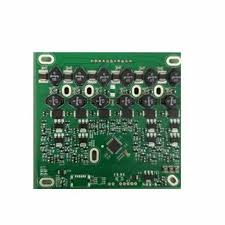
How to Minimize Signal Losses in RF PCBs
To minimize signal losses, RF PCBs must be designed with proper transmission lines. The type of transmission line chosen depends on the circuit’s specific needs and is based on factors like the width, thickness, and dielectric constant of each layer. These factors can affect the characteristic impedance of the line, which is measured in ohms and must be carefully controlled to prevent signal degradation. Microstrip, stripline, and coplanar waveguide transmission lines are all common options for RF PCBs.
The use of appropriate insulating materials is also critical. An ideal PCB material for RF applications has a low loss tangent, a low dielectric constant, and a low coefficient of thermal expansion. Polytetrafluoroethylene (PTFE) and Rogers laminate substrates are commonly used in RF PCBs due to their low loss properties at a wide range of frequencies.
Trace and component placement is also important. RF signals must be routed as close to the components as possible to minimize distance, which can result in loss and distortion. RF PCBs should also have enough ground planes to minimize parasitic capacitance and inductance. These planes must be adequately sized, without gaps or discontinuities, to protect against RF leakage into the circuit’s elements.
Insertion loss, which is the decrease in a signal’s strength as it travels through a component or a PCB trace, is also a significant factor. It is primarily due to resistance and capacitive losses and is directly proportional to the signal’s frequency and trace length. To minimize insertion loss, the PCB designer must choose suitable materials for each layer, optimize the trace width and thickness, and ensure that the signal path is properly insulated. In addition, the PCB should be built on a substrate with a low impedance value and a small via diameter.