

Typical aspect ratio for microvia buried via holes
In printed circuit boards (PCB), microvias are conductive holes used to connect layers within the board. Microvias are smaller than standard plated through vias, or PTV, which are regular holes that are drilled into copper and then filled with a conductive metal such as gold. They are most often used on high-density interconnect (HDI) PCBs.
The Institute of Printed Circuits (IPC) defines a microvia as a hole with a 1:1 aspect ratio and that doesn’t exceed 0.010 inches in depth. However, this is constantly changing as laser technology evolves, so it is important for designers to keep up with the latest microvia developments.
A microvia’s aspect ratio is important because it determines how well it can be plated. The lower the aspect ratio, the more reliable the via will be. It is recommended that the designer stay below a 2:1 aspect ratio to avoid problems with plating.
This is because drilling a hole at a higher aspect ratio could result in debris, drill smear, or inorganic fillers being deposited into the copper surface of the inner layer. These contaminants can cause interconnect defects, or ICDs. ICDs are common in PCB manufacturing, and can be caused by things like solder wicking down the via’s barrel or by the misregistration of the copper layers during lamination.
In addition, the larger the diameter of the plated hole, the less likely it will be to crack or delaminate. For this reason, it is important that the aspect ratio of the buried via hole is low enough to allow for proper etching and copper deposition.
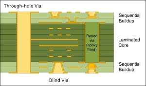
What is the typical aspect ratio for microvia buried via holes?
The aspect ratio of the buried via hole is also a factor in how it can be stacked to form a HDI PCB. Stacked microvias are simply stacks of buried vias, with each buried via connecting an outer layer to one or more inner layers. The stacked microvias are then infused with electroplated copper to form connections between the inner layers of the HDI PCB.
Stacked microvias can be arranged in a variety of ways, including staggered or stacked in rows. This allows the designer to take advantage of the metallurgical properties of different inner layers in the HDI stack. A staggered arrangement can also help to reduce the risk of failure of the stacked microvias at the interface between adjacent vias.
Another popular type of buried via is the V-shaped V-in-Pad (VIPP). This is a special kind of buried via that can be placed directly under pads for component leads on the PCB. This is a good option when a regular plated through via would interfere with the positioning of the component lead. However, it is important to note that a VIPP is not a substitute for a solder mask, which is required for all components on a PCB.
The main advantage of a VIPP is that it can be placed directly under the component pads. This reduces the number of steps needed to assemble the components, and can also improve the reliability of the assembly process because it can prevent solder from flowing down the via’s barrel and into the contact area.


